

Output shorts protection designs for LED driver ics
18-03-2015The non-synchronous, boost, power-conversion topology is often used in LED driver ics in applicationss where the input voltage (VIN) is insufficient to forward bias a series/parallel set of LED strings. This inductive switching topology creates the compliance voltage necessary to achieve LED current regulation and is commonly used in LCD backlighting applications. In applications where the LED matrix is remote from the driver - for example, automotive interior and exterior led lighting - the possibility of an output short to ground is real and can be a serious damage. A protection circuit that limits current and acts as an electronic circuit breaker can prevent terrible failures.
As illustrated in Fig. 1, the input of a boost converter is physically connected to its output through the boost inductor (L1) and boost diode (D1). Consequently, a short condition on the output can saturate the boost inductor and cause a current surge sufficient to damage the boost diode. Worse yet, the short can also disrupt everything connected to the input - including the pulsewidth-modulation (PWM) controller. Clearly, some form of circuit protection is necessary in using this topology to power remote LEDs. Lets consider a versatile and low-cost circuit that can be optimized to protect the boost converter and input from shorted load conditions. Moreover, we will present a circuit simulation that verifies the desired response.
Current limiter and electronic circuit breaker
The current shunt monitor (CSM) is a precision, high-gain differential current-sense amplifier often used to monitor input and output current. Fig. 2 illustrates the typical configuration. This particular device integrates an open drain comparator that can be programmed to trip, latch, and reset at a preprogrammed line current.
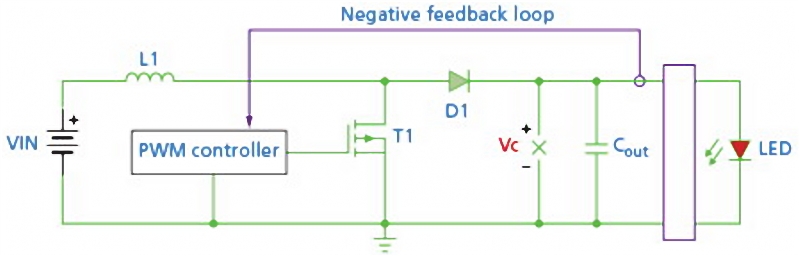
FIG. 1. An LED driver circuit based on the non-isolated boost topology.
The output of the comparator can be used to control an external MOSFET switch that can interrupt a load short within a few microseconds. In addition to interrupting input current under a fault condition on the output, the analog output can be used to address the so-called "negative input impedance" of a switching regulator that will cause input current to increase as the input voltage decreases.
Clamping the input can be achieved by connecting the input current with the output current in a logical "or" configuration. The goal is to create a composite feedback signal that drives the PWM controller as depicted in Fig. 3. The CSM then overrides the output current feedback and forces the LED current to decrease as the input voltage drops below a preset level, thereby limiting the input current.
Circuit operation
Fig. 4 illustrates the circuit implementation of a boost converter LED driver ic with output short-circuit protection. The Osram Opto Semiconductors Ostar LED shown in the circuit is a device for automotive LED headlamp applications and is actually a monolithic, five-die LED on an insulated metal substrate. The device has a surge current rating of 2A for less than 10 μs and a typical forward voltage of 18V at 1A. The DC/DC boost converter senses the forward LED current at the feedback pin and adjusts the output voltage greatly to regulate the LED current. The LED current is set by the sense resistor (RSNS) and its value is proportional to the internal bandgap reference of the PWM converter (RSNS = VREF/ILED). Using a boost converter with a low reference voltage improves higher converter efficiency and reduces component thermal stress.
Although inherently capable of achieving an operating life of over 50,000 hours, the LED is sensitive to temperature and electrical overstress and their dynamic impedance characteristic often challenges switching regulator component selection and control loop design. The challenges are documented in an application note. As such, a simulation of the circuit in Fig. 4 was developed to analyze the complexities of the LED driver ic/protection circuit and estimate circuit behavior under varied operating conditions.
The PWM controller chosen for this analysis has a feedback reference voltage of 0.26V. So, at 1A of LED current, only 0.26W is wastedd in the LED sense resistor. Because the CSM has a gain of 50, a much smaller-value sense resistor is used for sensing the output current. When the current through the CSM shunt resistor exceeds a programmed limit set by the CSM sense resistor, CSM gain and comparator threshold (R, R), the PMOS pass transistor interrupts load current - acting as an electronic circuit breaker.
The latched output can be reset by chaning the RESET pin low. However, for the purpose of this article, the RESET has been disabled to examine the speed of response. The response speed and peak currents depend on many variables. These include component selection, CSM bandwidth, noise filter, output capacitance, FET selection, and output boost inductor. Collectively, these factors affect the converter output impedance. To accurately assess behavior, we ran the simulation with a maximum time step set at 50 ns, and the DC relative tolerance set to 0.001%. The analysis was done in TINA-TI, a free Berkeley SPICE 3f5 compatible simulator. The 5-ms simulation of the boost converter operating at 300 kHz runs start-up to steady state in just under 30 seconds.
Where to place the CSM
The CSM can be placed on the input or output of the boost converter. In this simulation, the CSM is placed on the output where it senses current through a 10-mΩ shunt placed in series with the output PMOS pass element (T5). Depending on placement of the CSM, the circuit will protect against internal and/or external short conditions. However, the CSM must be designed with sufficient common mode range (CMR) under all operating conditions.
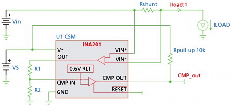
FIG. 2. A current shunt monitor component adds protection.
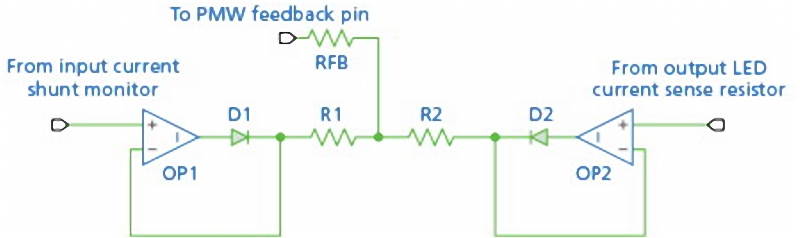
FIG. 3. The input current limiter relies on sensing input and output current.
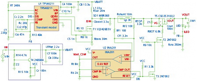
FIG. 4. The LED boost driver circuit with shorted load fault protection.
If placed on the input to the boost converter, a CSM with a lower CMR can be selected. However, placing the CSM on the output bypasses the boost inductor and shorten a faster reaction time to a short condition. Regardless of where the CSM is placed, an RC filter should be used to attenuate noise and resonance ringing that may occur as a result of unexpected di/dt events through the shunt resistor. A small 100Ω resistor and differential capacitor can be placed with a time constant three times larger than the estimated Lp/R time constant of the shunt where Lp is the parasitic shunt inductance. Since the gain error and bandwidth of the CSM is adversely affected by this noise filter, it is important to keep the filter value small.
Simulation results
The simulation result is presented in Fig. 5. Vg is the control voltage to the PMOS FET and is set at -6V under normal conditions. Optimization is necessary depending on the threshold voltage of the FET, gate charge, and saturation characteristics. Minimizing voltage on the gate can improve reaction time, and the pull-up resistor should be selected to minimize the interrupting period. Note that the input current and gate voltage are shown with a high gate charge (purple), and low gate charge (blue) MOSFET.
Evidently the lower gate charge device minimizes current seen at the input. Selecting a MOSFET and gate drive circuit to achieve the best response are important considerations, as is limiting the di/dt and satisfying the MOSFET safe operating requirements. These are complex design considerations not easily analyzed; therefore, they are best simulated and confirmed on the bench.
Professional test software is available on some oscilloscopes such as Tektronix products to calculate switch power loss against MOSFET safe operating curves. Simulation suggests a response less than 2 μs in duration, resulting in an input current of less than 6A before the current is interrupted. The selection of the interrupting FET will influence the peak input and output current. High-performance, hot-swap controllers driving high side NMOS devices are another option and able to achieve interrupting times of less than 250 ns. These devices are optimized for backplane hot card insertion but may provide a higher-performance solution than what has been demonstrated here.
Failure occured
The circuit presented and simulated interrupts and also limits the input/output current of a boost-converter LED driver ic under varied load conditions. The circuit was optimized for use in an automotive LED headlamp driver. We showed that achieving the best circuit response time necessitates careful analysis and component selection. Integrating these sensitivities into a comprehensive time-domain circuit simulation helps to understand circuit behavior over operating conditions and component selection.
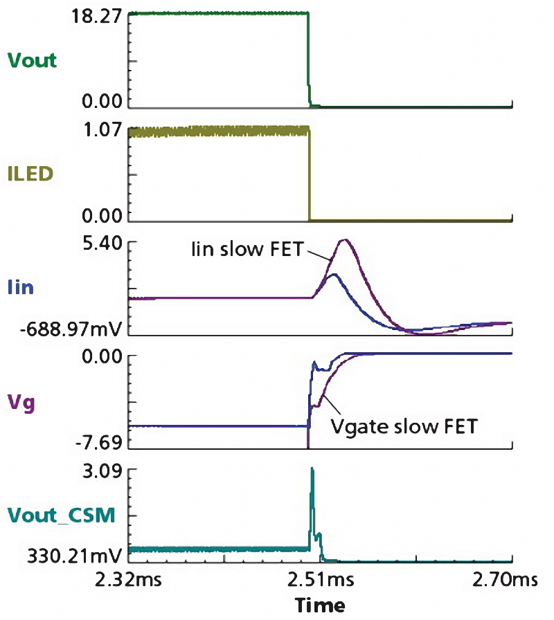
FIG. 5. Standard wired and wireless networks will carry the relatively simple commands and data passed between physical building systems and the building management devices.
Special-purpose hot swap controllers are available with specialized features and optimized performance and should be considered. In either case, careful analysis is necessary when implementing a circuit to interrupt or limit power. Designing a robust protection circuit for an LED driver ic is complex and software like TINA-TI, SPICE, and WEBENCH are helpful tools in accelerating the analysis and design.
©Copyright: 2008-2026 Guangzhou TEEHON Electronics Co., LTD. 